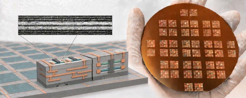
Researchers work out how to control 2D semiconductor growth for future chips
Researchers have demonstrated a way to control where 2D semiconductor crystals begin growing, potentially addressing an obstacle to manufacturing next-generation chips at scale, according to a study published in Nature. The paper, "Spatially deterministic nucleation of 2D semiconductors by etching flux," was authored by a team including researchers at KAIST and South Korean startup TDS Innovation and published on October 7. The technique uses an etching flux to suppress the formation of new crystals everywhere within each patterned growth region except at its geometric center. Two-dimensional materials are atomically thin rather than literally two-dimensional. Graphene, perhaps the best-known example, is a single layer of carbon atoms, but its lack of an intrinsic band gap makes it unsuitable for conventional switching transistors. Monolayers of some transition-metal dichalcogenides (TMDs), such as molybdenum disulfide (MoS₂), do have a band gap and are being investigated as materials for future transistors and other nanoscale devices. …
You're reading a preview. The full article is published by The Register on their website.
Read the full story on The Register