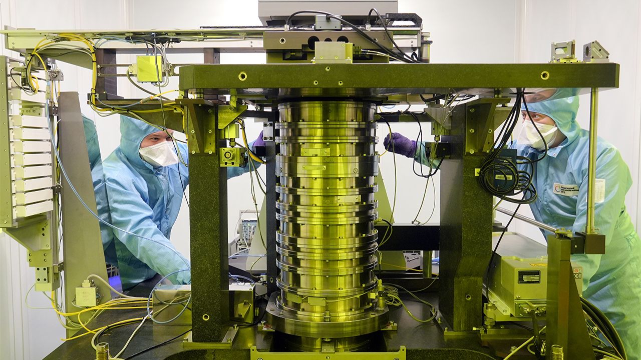
Russian firm completes country's first 130nm-capable chipmaking tool, trails modern equipment by 25 years
Russia-based Zelenograd Nanotechnology Center (ZNTC) has completed the third R&D stage of the company's first lithography tool capable of processing 200-mm wafers using a 130nm process technology, reports CNews. The tool is currently being tested internally and is years away from being used at a real fab to produce chips in mass quantities. Blogger Dmitrii Kuznetsov suggests that the device is the "first Russian 130nm-capable lithograph" that consists of components made in Russia. This may not be the case, though.
Go deeper with TH Premium: Silicon Photonics
Photonics and high-speed data movement is the next big AI bottleneck
Co-Packaged Optics (CPO) foundry roadmaps
Inside optical and the battle for scale – how the AI industry is racing to integrate photonic interconnects
How optical interconnects and silicon photonics emerged as AI's next hot commodity
Near-packaged optics (NPO) gains ground as the industry hedges against CPO's growing pains
"The creation of a prototype of a domestically developed photolithography system designed for a …
You're reading a preview. The full article is published by Tom's Hardware on their website.
Read the full story on Tom's Hardware