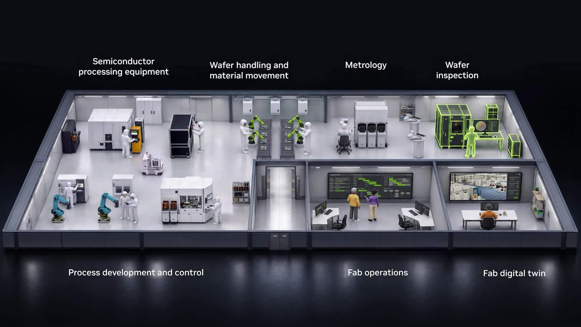
AI Is Changing How Semiconductor Fabs Work — and Engineers Are Moving Faster Because of It
Demand for advanced chips is rising. The processes to build them are getting more complex. And the margin for error is shrinking.
For engineers, understanding how a process change will behave, how a material will interact with a new step, how a defect maps back to a root cause are critical, challenging steps in semiconductor manufacturing — and these analyses can take days. Physical experiments on a fab line are slow and expensive. A wrong call on yield or process quality has real consequences.
AI is transforming semiconductor manufacturing, impacting what engineers can do — and how fast.
Accelerated computing shortens simulation time, allowing engineers to evaluate more alternatives before committing to physical trials.
Physics-based AI helps engineers predict process behavior without running a full simulation every time.
AI agents handle sequences of engineering tasks that once consumed hours.
And digital twins let teams test changes in a virtual environment before committing to physical trials.
Together, these capabilities describe an …
You're reading a preview. The full article is published by NVIDIA Blog on their website.
Read the full story on NVIDIA Blog

